Contribute
Register

G4 MDD Front Panel Pinout

Status
Not open for further replies.
Joined
Apr 23, 2016
Messages
18
Motherboard
Asus Pro Gaming Aura/Wifi ITX
CPU
i5 6900k
Graphics
Intel 530
Hi,

i want to do a MDD Mod and want to keep the FrontPanel. Is there a wireing diagramm to rerout the pins for a atx MB?

TIA
Thomas
P.S. pictures are welcome
 
Not sure if I have seen instructions for the MDD anywhere. I have only seen info for the Sawtooth and the Quicksilver. Reason probably being that the MDD are not popular among modders. Personally I have done a G5, a Q4 QS (info thread soon) and I am in the process of doing a G3 b&w. When I ordered a G4 MDD on EBay however I quickly realized what people mean when they say a MDD is basically impossible to mod.

Even without knowing your specific situation with the MDD my recommendation would be to ditch Apple's original front board and create your own with standard PC parts, which is what I did with the G4 QS. You basically re-create the front panel board holding the switches from wood or plastic. In my case I did a 3D print. You then use kits like this or this, if the front panel switches of the MDD have enough travel. The switches in the G4 QS did. The switches in the G3 b&w not so much though. There I created the front panel board with a 3D print and then soldered contact switches like this to an existing cable kit like the ones above.

Pictures of the 3D printed parts attached to this post. What you see there from top left to bottom left: 1) USB/audio front panel for the G4 Quicksilver, 2) holder for the flat contact switches + LED for a G4 QS, 3) holder for physical Lian Li switches for a G4 QS, 4) holder for flat contact switches + LED for a G3 b&w and G4 Sawtooth.
 

Attachments

  • IMG_20180531_141451.jpg
    IMG_20180531_141451.jpg
    397.1 KB · Views: 283
Last edited:
Thanks for your reply.

but i want to keep as much as possible from the interior and exterior .
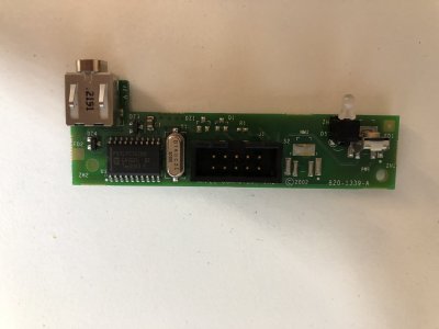
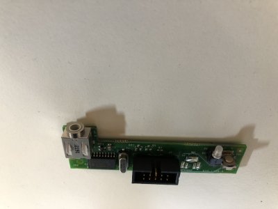
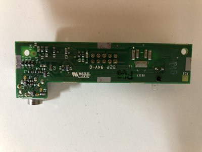
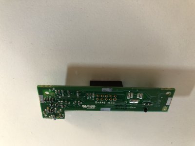
i made a few picture from the front panel, so if someone could get som information on it?? IMG_0547.jpg IMG_0548.jpg IMG_0549.jpg IMG_0547.jpg IMG_0548.jpg IMG_0549.jpg IMG_0550.jpg IMG_0551.jpg IMG_0552.jpg
 
I'm doing my own conversion. Are you able to post the 3D print files?
 
Last edited:
I will be soon doing the same kind of build and will be facing the same issue. If anyone has info on how to mod this power switch let me know, and if I find something I'll let you know !
 
I will be soon doing the same kind of build and will be facing the same issue. If anyone has info on how to mod this power switch let me know, and if I find something I'll let you know !

Might be a little too late, but the way I did it was to remove the chip and crystal and just solder the wires onto the back of the button itself.

Same with the LED.
 
Might be a little too late, but the way I did it was to remove the chip and crystal and just solder the wires onto the back of the button itself.

Same with the LED.
Thanks for the reply ! This is the next step I need to complete for my mod. I probed the board with my multimeter and came with the hypothesis that I could re-use the original cable and connector, and should have only one wire to solder on the board. See attached file, it is indicated by the red line I drew between the LED - and a pin on the connector that seems unused. The LED + and switch + are together on the same line, therefore I suppose I could bring only one positive signal from the motherboard. I already removed the chip and following your advice I will remove Y1 as well. Its been a few years since I did my electronics classes so if anyone could confirm or correct me before I do the operation it would be very appreciated !
Capture d’écran 2020-08-26 à 18.14.12.png
 
I tried to probe it but it started to annoy me. Ideally I could have done with some clips for my probes haha.
 
Status
Not open for further replies.
Back
Top